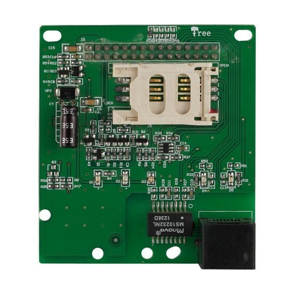
OEM Multilayer PCB Manufacturing Electronic Circuit Board Assembly
PCBA
♦ What's PCB Board Manufacturing Service?
PCB Manufacturing Service refers to the professional process of
producing Printed Circuit Boards (PCBs) based on customer
designs. PCBs are essential components in electronic devices,
providing mechanical support and electrical connections for
components like resistors, capacitors, and integrated circuits.
♦ What's PCBA Assembly?
PCBA Assembly (Printed Circuit Board Assembly) is the complete
process of mounting and soldering electronic components onto a bare
PCB to create a functional circuit board ready for integration into
a product.
♦ Key Features of PCB Manufacturing Service:
Customers provide design files (usually in Gerber format, along
with drill files, BOM, and assembly drawings).
Engineers review the design for manufacturability (DFM checks).
- PCB Fabrication Process
Material Selection – Choosing substrate materials (e.g., FR-4,
Rogers, flexible PCBs).
Printing & Etching – Transferring the circuit pattern onto
copper-clad laminate.
Layering & Lamination (for multi-layer PCBs).
Drilling & Plating – Creating vias and through-holes.
Solder Mask & Silkscreen – Applying protective coating and
component labels.
Surface Finish – Options like HASL, ENIG, OSP, or immersion
silver/gold.
Electrical Testing & Inspection – Ensuring no shorts or open
circuits (e.g., flying probe test, AOI).
- Additional Services (Optional)
PCB Assembly (PCBA) – Soldering components onto the board (SMT
or through-hole).
Testing & Quality Control – Functional testing, burn-in
testing, etc.
Box Build & Packaging – Full product assembly.
♦ Technical Parameters
Item | Specification |
Laers | 1~64 |
Board thickness | 0.1mm-10.0mm |
Material | FR-4,CEM-1/CEM-3,PI,High Tg,Rogers |
Max panel size | 32"×48"(800mm×1200mm) |
Min hole size | 0.075mm |
Min line width | 3mil(0.075mm) |
Surface finish | OSP,HASL,Imm Gold/Nickel/Ag, Electric gold |
Copper thickness | 0.5-15 OZ |
Soldermask | Green/Yellow/Black/White/Red/Blue |
Silkscreen | Red/Yellow/Black/White |
Min PAD | 5mil(0.13mm) |
Inter package | Vacuum |
Outer package | Carton |
Outline tolerance | ±0.75mm |
Hole tolerance | PTH:±0.05 NPTH:±0.025 |
Certificate | UL,ISO 9001,ISO14001,IATF16949 |
Special request | Blind hole+Gold finger + BGA |
Material Suppilers | Shengyi, KB, Nanya, ITEQ,etc. |


